
CMMB mobile digital TV terminal design
Designing a high performance CMMB mobile digital TV terminal requires a comprehensive consideration of many factors, which will be discussed in detail in this article.
This article refers to the address: http://
CMMB receiver chip
Zhuosheng Microelectronics' CMMB receiver chip MXD0251 integrates a self-developed silicon tuner and demodulator with 1.2V LDO. The external only needs 3.3V power supply, which reduces system cost and PCB area. The MXD0251 has a noise figure of less than 3.5dB over the UHF band; the carrier-to-noise ratio of the QPSK 0.5 mode is 1.4dB; the anti-digital analog adjacent-frequency interference performance is better than -50dB; the analog-to-analog same-frequency indicator reaches -14dB; Anti-co-channel interference uses advanced algorithms and has very good laboratory specifications, ensuring good reception sensitivity and anti-interference ability from the chip level. At present, in each city, the frequency of the transmitted signals is relatively high. In some places, the analog co-frequency and analog adjacent-frequency interference are very strong. The outstanding anti-adjacent interference performance and anti-interference interference performance of MXD0251 make it under these complicated conditions. Can achieve stable reception.
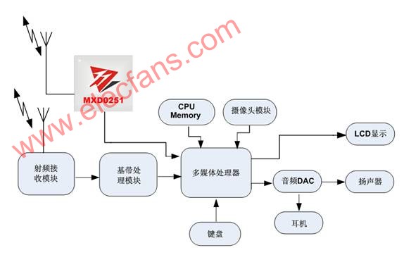
Figure 1: Architecture of the CMMB mobile digital TV terminal system based on MXD0251.
antenna
The signal chain starts from the antenna. At present, the CMMB receiving antenna of the mainstream handheld mobile terminal is a whip antenna, other ceramic built-in antennas, and an active built-in antenna also appear on the market. Take the whip antenna as an example. First, ensure the proper antenna length. Generally, the length is greater than 120mm and less than 200mm. The ideal length is 180mm.
After the antenna is determined structurally, it is necessary to perform matching debugging of the antenna. The purpose of antenna matching is to reduce signal reflection and improve signal transmission efficiency. For the UHF receive band, it is recommended that the antenna matching circuit reserve a network of the type. Good antenna matching should be such that the return loss is less than -6 dB in the operating band, the average gain of the antenna as a whole is greater than -4 dBi, and the average radiation efficiency is greater than 40. Data analysis is then performed based on the results of the active tests to determine if antenna matching needs to be modified to truly achieve matching conjugates or to purposefully optimize the performance of a particular band.
In summary, antenna matching can achieve performance balance in the entire operating frequency band, improve the overall receiving performance of the antenna, or optimize the performance of a certain frequency band. Figure 2 is a practical case. From the comparison of 500MHz and 700MHz, the 500MHz matching is better, the resonance is stronger, and the gain is 5dB higher than 700MHz.

Figure 2. Antenna passive performance.
After the antenna is selected, the RF receiving front end needs to be considered after the matching is completed. On the PCB, ensure that the RF traces are as short as possible, do not have extra fulcrums, there are no digital signals around the traces, there are no other non-ground vias, and RF grounding is sufficient. This is a basic requirement. Even with this, there may be various interferences coupled to the RF section. Zhuosheng Microelectronics has in-depth cooperation with mainstream CMMB antenna manufacturers, which can help customers choose the most suitable antenna solution, design a good matching circuit, and cooperate with antenna manufacturers to perform antenna matching debugging.
Board level interference
The influence of the power supply and the ground is mainly manifested by the deterioration of the noise floor of the system, so it is necessary to ensure a small power supply ripple. The CMMB is a time-slotted system. In the time slot of the received signal, the current will be relatively large, and the remaining time slots will have a small current. In this case, the voltage change needs to be considered. If it is DC-DC power supply, the layout trace should ensure that there is no interference in the power supply loop. In addition, the ground loop should ensure that the loop in the RF section is the shortest and clean. If there is a strong digital interference part, it can be split on the ground loop to reduce the impact of the digital part loop on the RF part.
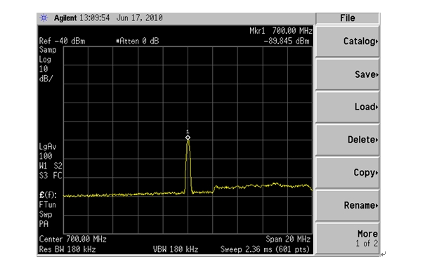
Figure 3 Single tone interference (Span: 20MHz)
The system clock, ADC, DAC, DDR clock, and some signal lines have the effect of interference, producing strong spurs (measured by the spectrum analyzer at the RF input) at certain multiplier points, as shown in Figure 3. Shown. The interference at 700MHz reaches -89dBm, which will reduce the receiving sensitivity at 698MHz. Sometimes, there are multiple spurs in the CMMB operating band, which means that multiple frequencies are affected, as shown in Figure 4.
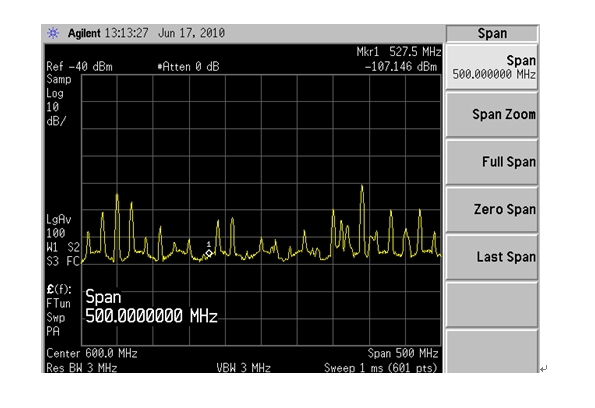
Figure 4 Multiple tone interference (Span: 500MHz)
The internal algorithm of MXD0251 has special treatment for the above situation, and it will automatically detect the position of spur and filter it out. Usually, these problems can also be avoided in the Layout. The interference source is far away from the RF part. In the ground loop processing, the interference source and the RF part are not directly connected to the RF trace layer, and the interference part is as short as possible. Of course, the phenomena encountered by various systems may be different, and specific phenomena need to be analyzed. Figure 5 is a system with excellent spur performance: there is no spur at each frequency point in the frequency band, thus making the sensitivity curve relatively flat.
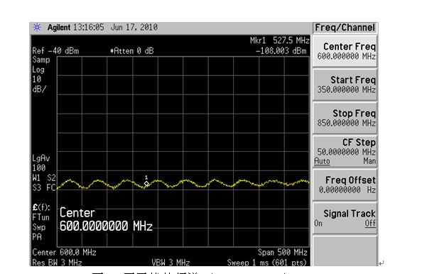
Figure 5 Interference-free spectrum (Span: 500MHz)
Coupled interference
Common coupling interferences include: radiated interference from LCD FPC; backlight interference from keyboard; DC-DC. Among them, the LCD is usually the main source of interference, and the noise is coupled to the inside of the chip via the antenna, which deteriorates the reception performance, and the interference of the screen often affects a wider frequency band. It is usually required to add EMI devices to the signal lines for shielding and grounding. From many cases, below 600MHz, the FPC of the screen will have an impact of 3dB to 7dB. The lower the frequency, the more affected. In addition, in the RF front end, it is necessary to pay attention to suppress interference of other wireless communication signals in the space, and adding a SAW filter is an effective solution.
In terms of coupled receiving sensitivity, good systems and poor systems sometimes differ by tens of dB, and such a gap will directly affect the success or failure of a mobile TV product design. Zhuosheng Microelectronics can provide closed-loop performance testing and open-loop performance testing for the customer's prototype, so that potential coupling interference in the whole machine can be found. We can identify the source of interference for the customer, analyze the interference factors, propose an interference suppression scheme, and debug the complete machine with excellent performance.