
Design of Switch Matrix for Broadband Low Crosstalk Video Based on AD8108
Design of Switch Matrix for Broadband Low Crosstalk Video Based on AD8108
Abstract: This paper introduces the design of a wide-band low-crosstalk video switching matrix. The matrix adopts the AD8108 of American Analog Devices as the signal switching chip of the wide-band video cutting matrix, and AT89C51 as the microcontroller to complete the matrix switching control and peripheral interface The video switching matrix maintained and maintained has the bandwidth capability of 325MHz and the characteristics of low crosstalk between channels, low in and out crosstalk, and a high in and out isolation of -98dB, which can fully meet the switching needs of high-performance video and VGA signals in various industries.
With the development of multimedia technology, the requirements for video switching in real-world applications are becoming higher and higher. In cable TV systems, high-quality video monitoring systems and large-screen display systems, high-quality video and VGA signals require a wide-bandwidth, low-interference switching matrix system to complete the switching process of the signal source. The previous switching matrix used mostly mechanical or electronic switch type, their shortcomings are usually the channel bandwidth can not pass the source of high-quality high-resolution car, and there is a strong crosstalk phenomenon.
1 AD8108 chip introduction
AD8l08 is an 8 × 8 high-speed non-crossover switch chip with a transmission bandwidth of up to 325MHz. The chip input port uses NPN differential input tube, and has a 150Ω resistor to buffer the input signal, plus non-blocking transmission, so that AD8108 can achieve high-performance video applications. The AD8108 has a gain flatness of 0.1 dB and a differential gain / differential phase error rate of 0.02% / 0.02 degree, while the crosstalk suppression is only -83dB. AD8108 can be switched through control signals input in serial or parallel. The output of serial port control data can be easily combined with multiple AD8108 chips to generate a larger-scale video switching matrix. The AD8108 chip can be used in a high-speed signal switching matrix to achieve the switching of composite video (NTSC, PAL, SECAM), component video (YUV, RGB), compressed video (MPEC, Wavelet), and HDB3 digital video. Usually the computer's VGA signal can be converted into five channels such as R, C, B, H, V, etc., and then switched by the switching matrix composed of AD8108. The channel switching time of the AD8108 chip is less than 25ns, and only less than 1% of the signal loss. 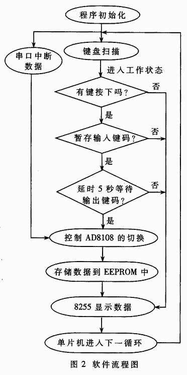
figure 1
2 Hardware principle of video switching matrix
The wide bandwidth and low crosstalk video switching matrix system is mainly composed of three AD8108 chips, two programmable logic devices ispMACH4A5 and an AT89C51 microcontroller. The 8 × 8 matrix switching unit is integrated inside the AD8108 chip, which is used to switch the input and output signals. Two ispMACH4A5 analog AD8] 08 chip switching process is used to switch synchronous digital logic. The AT89C51 chip is used as a micro-controller for switching control of each unit of the switching matrix and for forming a human-machine interface and building an RS232 serial communication interface.
The hardware schematic diagram of the video switching matrix system is shown in Figure 1. The three AD810S chips in the figure respectively complete the switching of 8 inputs and 8 outputs of R, G, and B signals. Rin [1-8], Cin [1-8], and Bin [1-8] represent R and G. 8 inputs with B signal. Rout [1-8], Gout [1-8] and Bout [1-8] represent the 8-channel output of R, G and B signals. There are two types of control for the AD8108 switching chip: serial input control and parallel input control. The AD8108 chip controls the switching of 8 inputs and 8 outputs through 32 registers in the chip. During serial input control. The D1 pin of the AD8108 is driven by the falling edge of the CLK pin signal, and sequentially transmits OUT7 [D3], OUT7 [D2] ... OUT0 [D1], OUT0 [D0] signals to the 32 registers in the chip. The register controls the input signal and The corresponding switching relationship of the output signal. The parallel input control is accomplished through the D0, D1, D2, and D3 signal pins and the A0, A1, and A2 signal pins. A0, A. 1. The A2 signal defines the output channel to be controlled. D0, D1, and D2 select the input switching channel corresponding to this channel, and D3 controls the opening and closing of the output channel specified by the A0, A1, and A2 signals. In AD8108, the / CE signal is used to select the chip. / RST is used to initialize the AD8108 chip, but this initialization does not initialize the contents of the register, but only initializes the output state of the switching matrix, so that all channel outputs are in a disabled state, and the switching logic in the register is still placed in a random arrangement Medium: / UPDATE signal is used to put the information in the register on the switching matrix, so that the set matrix switching logic works. The DO pin is used for serial control between multiple AD8108 chips. After the R, G and B signals are switched, the H and V signals can be switched by two programmable logic chips ispMACH4A5. Since the H signal and the V signal are synchronized digital logic signals, a digital programmable logic device with a rise time of 15 ns is used to complete the switching of the H and V signals to ensure the edge synchronization of the digital synchronization logic. Figure 1 ispMACH4A5 (1) to complete the 8 × 8 switching of the H signal, ispMACH4A5 (2) to complete the 8 × 8 switching of the V signal. The connection of S / PAR, CLK, DI, DO, / UPDATE, / CE, / RST, D [3: 0] and A [2: 0] signals of the ispMACH4A5 chip is consistent with the connection of the AD8108 chip, and it is also established in ispMACH4A5 The switching matrix logic consistent with the AD8108 logic is introduced. AD8108 is connected with the / CE signal in ispMACH4A5 to bind R, G, B, H, and V together to control the five-way signal R, G, B, H, and V of the VCA signal. Of course, R, G, B, H, and V can be controlled separately to form more combinations and finer switching.
In Figure 1, AT89C51 is used to switch the AD8108 and ispMACH4A5 chips. Pl0 to P15 are buffered by 74F244 to form CLK, S / PAR, DI, / UPDATE, / CE and / PST and then connected to the corresponding pins in the AD8108 and ispMACH4A5 chips. The P20 to P26 pins are buffered by the 74F244 chip and then connected to D0, D1, D2, D3, A0, Al, A2 of the AD8108 and ispMACH4A5 chips. P0 port and ALE / P pin of AT89C51. Connect with 8255 chip through 74F373. PA port, PB port and PC port extended by 8255 are used for keyboard input and LED display control. The AT89C51 also connects the TXD and RXD pins to the TX1 and RX1 of MAX232, and expands the serial port to facilitate the remote computer to control the switching logic of the switching matrix system through the serial port. AT89C51 is also connected with the watchdog circuit and E2PROM module in the X5045 chip to complete the monitoring and control data storage of the MCU.
3 Software flow
The software flow chart is shown in Figure 2. After the hardware system powered by 5V is powered on, the system is first initialized. Here, AT89C51 completes the initialization of reading and writing to the serial port and E2ROM chip; 8255 chip completes the initialization of keyboard scanning and display; and / RST of AD8108 chip completes the initialization of the switching matrix. Then AT89C51 reads the switching logic saved in X5025 E2ROM during the last power-off and sends it to the register in AD8108 chip and ispMACH4A5 chip through DI serial control port, when their / UPDATE pin is added a low level, then The logic at the last power-off plays a role in the AD8108 and ispMACH4A5, thereby forming input and output switching logic; later the software enters the cycle of scanning the keyboard and serial port interruption. Because the switching matrix system displays LEDs using a dynamic display method, when receiving serial port interrupt control signals and keyboard input control signals, the parallel control method is generally used to switch the AD8108 to save switching processing time. Of course, on other occasions, if the matrix is ​​switched on a large scale, the DI serial control can be more convenient and faster.
4 Performance analysis of video switching matrix
In high-speed video switching matrix systems, bandwidth and crosstalk are two important metrics. AD 8108 chip adopts input buffer and high isolation operational amplifier to achieve low crosstalk performance; adopts non-blocking design structure to achieve wide bandwidth performance of chip system and achieve low energy consumption. The -3dB bandwidth of the video switching matrix system composed of AD 8108 chips can reach 325MHz.
The problem of crosstalk can generally be defined as the interference of signals between channels transmitted in the same direction. It can also be defined as the coupling interference between the entry and exit of a system. In the video switching matrix system, the process of crosstalk is complicated, and there is electric crosstalk. For example, each resistor is an electromagnetic transmitter and an electromagnetic receiver; there is magnetic crosstalk, and the flow of current will generate a magnetic field and then other Crosstalk voltage is generated on the line; there is also common resistance feedback crosstalk, which refers to the crosstalk formed by the common line resistance due to the common power supply line and the ground line or other common wiring. All these crosstalks are combined by vectors to form a complex vector variable. The method to reduce crosstalk is to select a chip with low crosstalk, and to suppress crosstalk in the system design. In this system, the crosstalk between channels is more obvious. The general formula for measuring crosstalk between channels is as follows:
Among them, s = jw is the amount of Laplace conversion, Atest (s) is the amplitude of the crosstalk signal in the selected channel, and Atest (s) is the amplitude of the test signal. If the crosstalk value between channels is expressed in dB value, you can see that ︱XT︱ is a frequency-dependent quantity, and has nothing to do with the amplitude of the test signal. In addition, there is a phase correlation between the crosstalk signal and the test signal. According to the relevant definition of crosstalk, a test environment can be established to measure the relationship between crosstalk and frequency. As shown in Figure 3, let IN3 be grounded through a 75Ω resistor, and the other 7 lines input 1V standard voltage test signal Atest (s), and the frequency of the test signal can be adjusted, and the output of these 7 channels is also through 75 To the ground. Then measure the amplitude Asel (s) of the OUT3 output link signal. According to formula (1), the level of crosstalk between channels can be calculated. Change the frequency of the input test signal to continue the crosstalk test, you can get a frequency-dependent crosstalk change graph, as shown in Figure 4, generally speaking, due to the obvious interference characteristics of high-frequency signals, crosstalk will follow the frequency It becomes higher and gradually increases. Here, the crosstalk of the 7-channel input to the single-channel signal is measured. When the crosstalk of one channel to another channel is to be measured, this test method can also be used.
In order to solve the problem of crosstalk, a number of measures have been adopted in the design to ensure. The PCB layout of the five signals of R, G, B, H and V is arranged in parallel. A better method is to arrange them on different boards; in addition, to do a good job of power supply filtering, use high-throughput filter capacitors at the power terminals of each chip to filter, and the filter capacitors should be as close as possible to the chip The power supply terminal; In addition, the input and output terminals of R, G, B are grounded with a 75Ω resistor to match the external 75Ω video connection resistance. 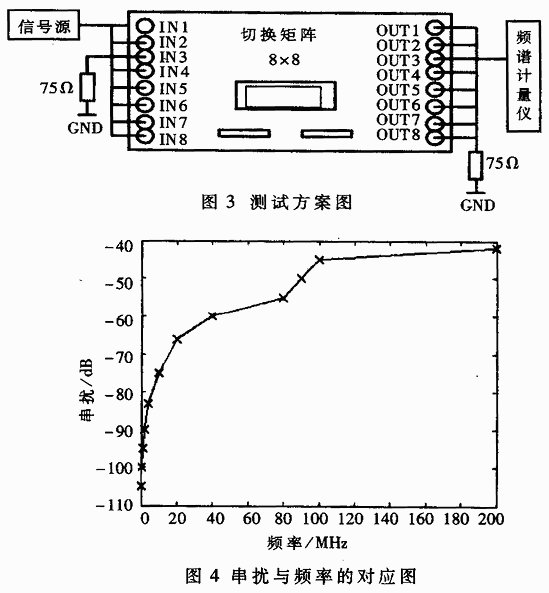
5 Application analysis
The high-performance matrix switching system based on AD8108 can be applied to cable TV systems, large-screen display systems, and computer monitoring systems. Its 325MHz channel bandwidth can realize the non-destructive switching of the true color SXGA signal with a resolution of 1280 × 1024, 75Hz and 24bit in the computer application system. In the high-resolution large-screen display system, it is necessary to switch the computer source signals of different resolutions to the large-screen display. The switching matrix based on the AD8108 can effectively complete such a switching process. During implementation, the chrominance signals and synchronization signals of the VGA signal of the computer are generally decomposed into R, G, B, H, and V signals, and then switched to the display projector through the switching matrix based on the AD8108. In addition, the serial control input and output chain function and output prohibition function of the AD8108 chip can also make multiple AD8108s form a switching matrix of 16x8, 16x16 or more input and output ports. The input can use parallel input, and the output can use line and mode, which can effectively achieve a larger-scale broadband switching matrix with low crosstalk.
Stainless Steel Coffee Urn,Catering Coffee Urn,50 Cup Coffee Urn,Mechanical Coffee Urn
FOSHAN FORTUNE ELECTRICAL APPLIANCE CO.,LTD , https://www.coffelady.com