ESD protection design for mobile phone interface
Almost all chipsets currently have on-chip ESD protection. The ESD circuit is placed on the periphery of the chip and adjacent to the I/O pads, which are used to protect the chipset during wafer fabrication and back-end assembly processes. In these environments, ESD can be introduced to the chipset through equipment or plant line workers. Key ESD specifications include Human Body Model (HBM), Charged Device Model (CDM), and Machine Model (MM). The purpose of these test specifications is to ensure that the chipset maintains high manufacturing yields in the manufacturing environment.
This article refers to the address: http://
Traditionally, chip manufacturers have been trying to maintain the 2,000V level required by HBM. From a cost-benefit perspective, this has proven to be a difficult task. As can be seen from Figure 1, as the manufacturing technology shifts to below 90 nm, the cost of maintaining the ESD protection level at 2,000 V has begun to increase exponentially. Therefore, the new goal now is to reduce the level of ESD protection on the chip, but maintain the same high manufacturing yield level.
The currently accepted critical ESD protection voltage level is approximately 500V. At this level, the cost of the chip is increased more reasonably, and the yield level will not be damaged. This is because typical fabs and assembly plants have policies that limit ESD to 500V or less.
Therefore, even if all chipsets contain some ESD protection circuitry on the die, the goal is simply to ensure high yields. However, this level of ESD protection is not enough to protect the chipset from the serious ESD events that consumers will encounter when actually using the phone. In a consumer environment that cannot be controlled in advance, different ESD protection specifications must be used. This is IEC61000-4-2.
This IEC specification has been used by many application manufacturers (mobile phones, smart phones, MP3 players, etc.) to ensure that their products work reliably and without early failure. This specification has a much higher ESD protection voltage level and is therefore not compatible with HBM. The tests required by the HBM specification are concentrated at 500V. On the other hand, the air discharge method in the IEC requires tests exceeding 15,000V.
This means that there is a very large gap between the level of testing required for the ESD protection capabilities of the chipset and the reliability of the application. This usually means that board-level ESD components such as multi-layer varistors, polymer ESD suppressors and silicon protection arrays must fill this gap. One thing to note is that the ESD protection performance of these technologies is different. Specifically, the on-time and clamp voltage vary widely. This means that for sensitive chipsets, applications that use one of these technologies cannot pass ESD testing, but can use ESD testing when using another technology.
The most common board-level ESD protection devices in the industry currently have the following three types, and their key attributes are as follows.
Multilayer varistor (MLV): This type of zinc oxide based device provides ESD protection and low level surge protection. Their small form factor (down to 0402 and 0201) makes them ideal for portable applications such as cell phones and digital cameras.
Silicon Protection Array (SPA): These discrete and multichannel devices are designed to protect data lines and I/O lines from ESD and low-level transient surges. Its key feature is the very low clamping voltage, which allows them to protect the most sensitive circuits.
Polymer ESD Suppressor (PGB): This is the latest technology designed to produce the smallest parasitic capacitance value (<0. 2pF). This feature allows them to be used in high speed digital and RF circuits without causing any signal degradation.
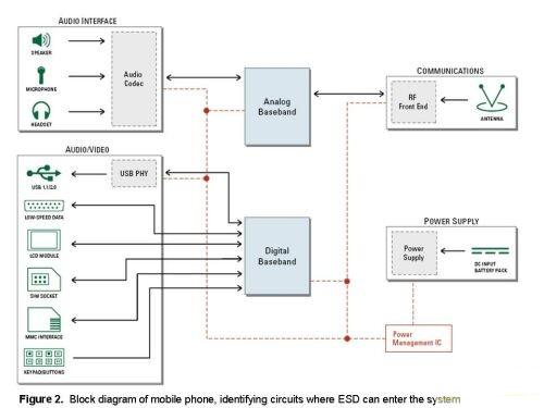
Since the phone is designed for mass consumers and can be used in any environment, it is very likely that ESD will enter one of the ports or I/O interfaces and cause the chipset to be electrically unstable or completely damaged. Figure 2 is used to help illustrate what ESD protection techniques should be used for different circuits. It shows that all circuits have the potential to provide a way for ESD to enter the phone.