
GAL-based I2C bus timing simulation
The FI1200 MK2 Series TV Signal Front End Processor is designed by Philips for RF applications in a computer multimedia environment. The FI1256 MK2 is a model in this series. It is small in size, compact in structure and stable in performance. It can demodulate video signals and audio signals directly from RF signals, and requires only a single 5V power supply. It can be received and wired on teletext. Many occasions such as automatic monitoring of television signals have been widely used. I have used it to develop a variety of equipment such as teletext receiver cards and TV signal detection systems.
The FI1256 MK2 can be programmed via the I2C serial bus interface. When using a microcontroller for program control, a microcontroller with an I2C interface can be directly connected to the FI1256 MK2. A microcontroller without an I2C interface can simulate the timing of the I2C bus with an I/O line. However, when FI1256 MK2 is used in a computer expansion card, in order to save cost, when programming directly through the bus of the computer, it is necessary to simulate the timing of the I2C bus by using the bus of the computer. This paper presents a method for controlling FI1256 MK2 with programmable logic device GAL and ISA bus analog I2C bus timing. This method is similar to the method in which the PCI bus is simulated.
1 I2C bus operation mode
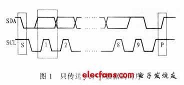
The I2C bus is a widely used serial multi-master bus that allows multiple devices with control bus capabilities to be connected to the bus. The I2C bus transfers data to devices connected to the bus through serial data (SDA) and serial clock (SCL) lines. The identification of each device is determined by a specific address. In addition to being a transmitter and receiver, the device can be configured as a master and a slave. The master is used to initiate data transmission on the bus and generate the clock signals required for data transfer. All other addressed devices are considered to be controlled. Both the SDA line and the SCL line are bidirectional transmission lines that are each connected to a positive supply via a pull-up resistor. Both lines are high when the bus is idle. The device output stage connected to the bus must be open-collector or open-drain to create a "wire-and-wire" function that facilitates access by multiple devices. In the standard mode, the data transfer rate on the I2C bus can reach 100kbps, and in the fast mode it can reach 400kbps. The number of devices connected to the bus is limited by the 400pF bus capacitance. During data transfer, the data on the SDA line must be stable during SCL high. Only when the clock signal on the SCL line is low, the state on the data line can be changed. When the SCL line is held high, the high-to-low and low-to-high level changes on the SDA line are usually defined as start and stop conditions, respectively. When the master initiates data transfer, it always gives the start condition first, then transfers several bytes of data, and finally gives a stop condition to end a data transfer process. Figure 1 shows the bus timing for transmitting only one byte with start and stop conditions.
2 Analog I2C bus timing
Programmable logic devices are a branch of ASICs that have been developed over the past two decades and are ideal for designing new digital systems. Not only is it fast, it has high integration, it has user-definable logic functions, some can be encrypted, and can be reprogrammed. Therefore, it can not only adapt to various application needs, but also greatly simplify the hardware system and reduce costs. Improve the flexibility, reliability and confidentiality of the system, so it has developed rapidly in recent years. Among the various programmable logic devices, CPLD is the most powerful, but the price is higher and the use is more complicated. GAL not only has quite strong functions and flexibility, but also easy programming control (can use ordinary programmers), the price is very low, close to general-purpose integrated circuits, so the use of GAL in systems where digital logic is not very complicated is very suitable.
When programming the FI1256 MK2 with the computer's ISA bus, the FI1256 MK2 can be used as a peripheral, and then the SCL and SDA can be simulated with two data lines. It should be noted that due to the high speed of the computer and the short bus cycle, the timing requirement of the I2C bus cannot be reached. Therefore, the delay should be performed after the bus cycle, so that the high-impedance state on the bus or the communication data with other devices will be Destroy the timing of I2C, so the state of SDA and SCL should be latched to meet the timing requirements of the I2C bus. Figure 2 shows the design of the ISA and I2C interface circuit using GAL. Since the operation of the FI1256 MK2 is generally only a write programming control byte, for simplicity, this circuit is only used to implement the write operation timing of the computer as the master.
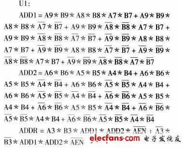
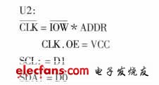
In Figure 2, the DIP switch K is used to set the address of the FI1256 MK2 as a computer peripheral. U1 is used to decode the address when the computer accesses the peripheral. U2 is used to simulate the I2C with the two data lines of the ISA bus. Bus timing. The two GAL logic equations (written in FAST-MAP format) are given below, and the functions implemented by the circuit are briefly described in relation to the equations.
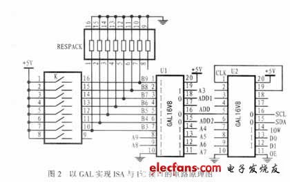
Through the above equation, U1 can complete the decoding function of the address. When the peripheral address appearing on the ISA bus matches the address set by the DIP switch, it will get a high level on its address valid output terminal ADDR. Since the GAL can only have a maximum of 8 entries, the two intermediate operations of ADD1 and ADD2 are used in the equation, and they are used as feedback signals to be re-introduced into the input inside the GAL. The AEN signal is used to mask the address that appears on the bus during the DMA cycle.
The U2 clock signal is introduced by the address ADDR and the peripheral write signal IOW to eliminate the signal on the bus that accesses the memory while latching the data with its rising edge. SCL and SDA can be simulated with data lines D0 and D1, respectively. When a peripheral write cycle has elapsed, the data for D0 and D1 will be latched on SDA and SCL, and will not change until the next peripheral write cycle to the same peripheral address. This allows the timing of the I2C bus to be obtained by intermittently outputting data on the two data lines D0 and D1.
By analyzing the data transmission format given in Figure 1, the transmitted data stream can be divided into three transmission states, namely, the transmission start signal, the transmission termination signal, and the transmission of one byte (with an acknowledge bit followed). Different data processes only differ in the number of data bytes written. As long as the simulation software can implement the above three transfer states, it can simulate any master write operation. Therefore, the above three transfer states can be implemented separately by the following subroutine.
The cold fog is a new fan product. Cold fog fan and ordinary fan is different, even if the temperature and then high, cold fumes blow out must be cold. Cold fog fan in the bottom of the water tank connected to the power, the cold fog began to turn, slightly braved the fog, people feel cool.
Cold fog fan third gear speed, 90 minutes timer, water tank filled with water, the cold fog fans not only cool faster, but also can purify the air, both practical and environmentally friendly. Cold fog fan with optimized fan structure, stable operation, with a large amount of air, low noise, beautiful and so on.
Mist Fan
16 Inch Water Mist Fan,Coolers Devices,Ventilation Devices
Ningbo APG Machine(appliance)Co.,Ltd , http://www.apgelectrical.com