
High speed connection requires RS-485
Thomas Kugelstadt, Intersil Corporation
RS-485 is a physical layer standard for many industrial communication systems (eg PROFIBUS systems), or for connection devices such as PLCs, SCADA systems, RTUs or MODBUS systems. As shown in Figure 1, high-speed and ultra-high-speed RS-485 data links typically use relatively simple configurations such as single or parallel point-to-point (full-duplex or half-duplex) or multi-drop configurations.
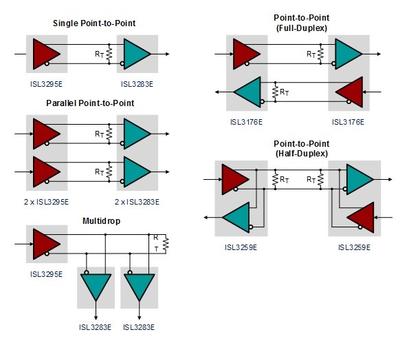
Figure 1. Typical configuration of a high-speed RS-485 link
These simple diagrams imply many design considerations such as transceiver selection, board layout for each node, cable selection and interconnect geometry, and more. To meet end-user requirements for higher data rates and longer cables, and to ensure that identifiable data errors are minimized, all of these aspects must be considered and optimized. This article discusses key design considerations that engineers should consider during high-speed data transfers and provides general design guidelines and cabling recommendations through a bus node design example.
Signal degradation (shown as signal jitter) is a major factor that limits the actual cable length. This signal jitter is the result of driver and receiver pulse offsets and pattern-dependent cable skew. The driver and receiver pulse deviation is the difference between the propagation delays of the rising and falling edges of the driver and receiver.
The bit pattern-dependent cable skew is a variation of the bus signal's rise and fall times, which is caused by different bit sequences. Data pulses respond to bit pattern-dependent offsets by loss of amplitude, rounded edges, time shifts, and pulse "smearing" at neighboring bit intervals.
Using data encoding methods such as Manchester, 8b/10b or 33hex helps to reduce jitter. Encoding the data stream introduces a transition in the data stream, which results in a more balanced cable charge and discharge and a more consistent signal amplitude. However, data encoding can shorten the charging and discharging time of the cable capacitance, thereby reducing the bus signal amplitude.
Transceiver selection
To provide the receiver with a reliable input signal, it is recommended to use a high-speed transceiver with a large differential output voltage (VOD) and low offset. Large VODs can overcome signal attenuation caused by cable attenuation, data encoding, and common-mode loading, and ensure adequate noise margin at the remote receiver input.
For low-voltage designs, it should be noted that the output stage of a so-called "affordable" 3V transceiver can only provide output voltages that conform to the RS-485 standard at supply voltages above 4V. In the case of lower supply rails, the transistor efficiency drops dramatically, making VOD 40% lower than the 1.5V minimum required by the RS-485 standard. Such a low output voltage does not generate enough noise margin to trigger the remote receiver.
The lowest VOD range for Intersil's high-speed transceiver family with very high output drive capability is 160% of the minimum value of 1.5V (4.5V supply voltage) to 100% (3.0V supply voltage), providing true 3V RS-485 drive capability . Typical VODs measured at the maximum operating temperature exceed 27% of the RS-485 standard in the case of a 3V transceiver and 70% to 93% in the 5V transceiver case.
In addition, the small pulse offset minimizes the transceiver's share of the total jitter budget for the data link. All Intersil high-speed transceivers have a maximum pulse offset of 1.5 ns. Moreover, the offsets of different parts (which also need to be considered in synchronization applications) are less than 4 ns.
Bus node design
The bus node shown in Figure 2 contains a transceiver, an FPGA-based controller, an anti-surge resistor, and a transient suppressor for lightning protection. Transceiver Pinout Place the bus terminals (A/Y, B/Z) on one side of the IC and the single-ended data lines (DI, RO) and control lines (DE, /RE) on the other side, simplifying design.
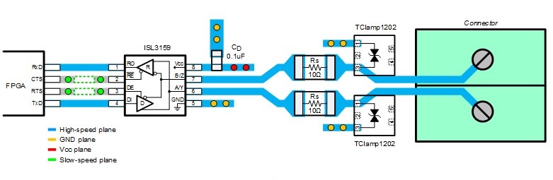
Figure 2. Major components and interconnections
In order to minimize electromagnetic interference, controlled impedance transmission lines must be deployed. On the bus side, the differential impedance of the bus trace must match the characteristic impedance (100Ω or 120Ω) of the transmission medium. On the control side, the line impedance of the single-ended trace is usually set to 50Ω.
In a simple bus node consisting of a transceiver and a controller, the relative length, width, height, and pitch of the traces can be carefully selected, as well as by the close electrical coupling with the low inductance reference plane (ground plane or power plane). Implement controlled impedance transmission lines. The length of the differential signal trace between the controller and transceiver connection traces and the transceiver and cable connectors must be calculated. In the case of each connection, the electrical length should be shorter than 1/10 of the rise time of the driver output. This relationship can be expressed as follows:
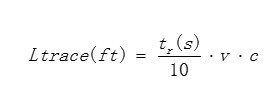
Where: Ltrace is the trace length in feet tr is the drive rise time in seconds v = signal speed in percent of the speed of light c = speed of light in 9.8 x 108 feet per second
For adjacent single-ended lines above the ground plane, such as the recommended line for connecting the controller to the transceiver, the relative signal speed is 56%. Using the 2ns ISL3159E rise time, the maximum trace length can be calculated as 33mm.
The trace length from the transceiver to the cable connector can be calculated as the relative signal speed (ie, 40%) of the traces on the standard FR4 substrate. In this case, the calculated maximum trace length is 24mm.
The lightning arrestor shown in Figure 2 can complicate the design. You can use the Field Solver software tool to accurately calculate the required trace geometry. The software calculates characteristic impedance, signal speed, crosstalk, and differential impedance, and allows the user to evaluate virtually any geometric shape. In addition to considering first order terms such as line width, dielectric thickness, and dielectric constant, second order terms such as trace thickness, solder mask, and trace etchback can also be considered.
In PCB design, in order to minimize electromagnetic interference, at least four layers are required. These layers should be stacked in the order shown in Figure 3. The top layer is the high-speed signal layer, then the ground layer and the power plane, and the bottom layer is the control signal layer.
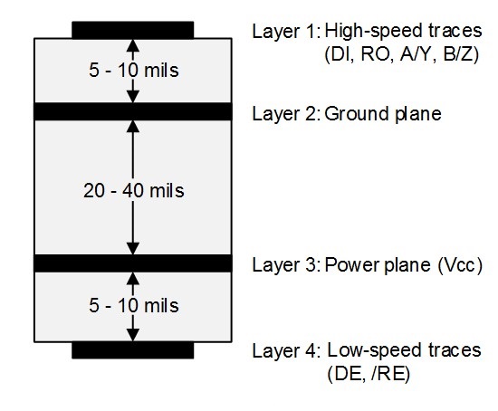
Figure 3. Recommended 4-layer PCB structure
The scheme of arranging high-speed traces on the top layer helps to avoid the additional complexity and inductance associated with adding vias while allowing high-speed single-ended data lines from the bus connector to the transceiver bus terminal and from the transceiver The interconnection to the node controller is cleaner.
Placing the solid ground plane underneath the high-speed signal layer establishes the controlled impedance required for the transmission line interconnection and provides a low-inductance path for the return current. Placing the power plane underneath the ground plane can create additional high frequency bypass capacitors.
Placing lower speed control (enable) signals on the ground provides more flexibility. These signal chains typically have tolerances for discontinuities (such as vias), and this separation almost eliminates crosstalk from high-speed data traces.
Six general guidelines that should be followed:
Use signal trace vias and connector pads as small as possible to minimize their effect on differential impedance;
Use a solid power plane and ground plane to control the impedance and minimize noise on the transceiver power line;
Keep trace lengths between the RS-485 connector and transceiver as short as possible to minimize attenuation and reflections;
Place a large capacitor (such as 10μF) close to a power source (such as a regulator) or place it on the PCB;
Place 0.1μF and 0.01μF small decoupling capacitors on the VCC pins of the transceiver to provide local charge sources for ICs that require large currents for internal switching;
If vias are required, multiple vias can be used when connecting Vcc, GND, decoupling capacitors, and TVS diodes to high speed ICs.
In addition, the following recommendations for cable selection, bus termination, and management short-term help to complete the design from a system perspective.
Transmission cable
The RS-485 standard recommends using the nominal characteristic impedance Z0 = 120Ω unshielded twisted pair (UTP). The commonly used cable is a dedicated single-pair RS-485 cable with Z0 = 120Ω, or a five-wire cable with four signal pairs and Z0 = 100Ω.
When using a Cat5 cable in a single-pair application, the three unused signal pairs should be properly grounded using a resistor of RT = 100Ω across the cable, which prevents noise from unused wires from entering the data pair.
Please note that when selecting multiple pairs of cables other than Category 5 cables, the so-called “offset-free cable†cannot be used. This type of cable is designed for analog signals with lower or zero harmonic content. Using such cables for data signals can cause large crosstalk and data errors.
Bus termination
Because the RS-485 standard allows the use of two termination resistors, high-speed data lines should always use termination resistors RT at both ends of the data link. The value of RT should match the characteristic impedance of the cable Z0 or the impedance of the controlled impedance transmission line on the circuit board RT = Z0 = 100Ω.
Short stub length
The connection between the transceiver and the main data cable (called the short line) does not need to be terminated to avoid bus overload. On the other hand, the stub length should be as short as possible to prevent signal reflection. The daisy-chain cable connection method effectively reduces the stub length to the PCB trace length from the transceiver to the connector, which can be calculated using the simple formula above or Field-Solver software for node design.
to sum up
Applying sound design principles at board and system level, and using transceivers that provide high output drive capability and minimum skew at both 3.3V and 5V supplies, can help designers overcome signal degradation in RS-485 high speed communication links problem.
Shenzhen Chaoran Technology Corp. , https://www.chaoran-remote.com