
PCB double-sided reflow process (SMT) introduction and precautions
At present, the mainstream circuit board assembly technology in the SMT industry should not be "full-flow reflow soldering". Others, of course, have other board soldering methods, and this full-board reflow soldering can be divided into single-panel reflow soldering and Double-panel reflow soldering, single-sided reflow soldering of the board is now rarely used, because double-sided reflow can save board space, which means that the production can be made smaller, so most of the boards seen on the market It is a double-sided reflow process.
(Off-topic, if there is no space limitation, in fact, the single-panel process can save one SMT process. If the material cost is compared with the SMT's working cost, maybe the single-panel is more cost-effective.)
Because the "double-sided reflow process" requires two reflows, there are some process limitations. The most common problem is that when the board goes to the second reflow oven, the parts on the first side will be Dropped by the gravity relationship, especially when the board flows to the high temperature of the reflow zone of the furnace, this article will explain the precautions for the placement of parts in the double-sided reflow process:
(A second question, why did most of the small parts that had been tinned on the first side not fall back and melted when the second side passed the reflow oven? Why are the more heavy parts falling?)
Which SMD parts should be placed on the first side of the reflow oven?
Generally speaking, the smaller parts are recommended to be placed on the first side of the reflow oven, because the deformation of the PCB will be smaller when the first side passes through the reflow oven, and the precision of the solder paste printing will be higher, so it is more Put smaller parts.
Second, the smaller parts do not risk falling when the second reflow oven is over. Because the first surface part will be placed directly on the bottom surface of the circuit board when facing the second side, when the board enters the high temperature of the reflow area, it will not fall off the board because of excessive weight.
Third, the parts on the first panel must pass through the reflow furnace twice, so the temperature resistance must be able to withstand the temperature of two reflows. The general resistance and capacitance are usually required to be reflowed at least three times. In line with the requirements of some boards, it may be necessary to go back to the soldering furnace again because of the maintenance relationship.
Which SMD parts should be placed on the second side of the reflow oven? This should be the focus.
Large components or heavier components should be placed on the second side to avoid the risk of parts falling into the furnace when the furnace is over.
LGA and BGA parts should be placed on the second side of the furnace as much as possible, so as to avoid the unnecessary risk of re-soldering during the second pass to reduce the chance of empty/false welding. If there are small and small BGA parts, it is not recommended to place them on the first side of the reflow oven.
It is always controversial to place the BGA on the first or second side. Although the second side can avoid the risk of remelting the tin, the PCB will be deformed more often when the second side passes through the reflow oven. On the contrary, it will affect the quality of tin, so the work bear will not say that the BGA can be considered to be placed on the first side. But conversely, if the PCB is severely deformed, as long as the fine parts are placed on the second side, it must be a big problem. Because the position of the solder paste and the amount of solder paste will become inaccurate, the focus should be Find out how to avoid PCB distortion, instead of considering the BGA on the first side because of deformation, isn't it?
Parts that cannot withstand too many high temperatures should be placed on the second side of the reflow oven. This is to prevent the parts from being damaged by too many high temperatures.
PIH/PIP parts should also be placed on the second side of the furnace, unless the length of the solder fillet does not exceed the thickness of the board, otherwise the foot that protrudes from the surface of the PCB will interfere with the steel sheet on the second side, which will make the second side Solder paste printed steel plates can not be flat on the PCB, causing abnormal solder paste printing problems.
Some components may have soldering inside. For example, a cable connector with an LED lamp must pay attention to whether the temperature resistance of the component can pass through the reflowing furnace twice. If it is not possible, it must be placed on the second surface.
Only when the parts are placed on the second side of the patch to pass the reflow oven, it means that the circuit board has passed the high temperature baptism of the reflow oven. At this time, the circuit board has some warpage and deformation, that is, tin. The amount of paste printed and the position of printing will become more difficult to control, so it will easily cause problems such as empty welding or short circuit. Therefore, it is recommended to place 0201 and fine feet in the parts of the second side. For pitch parts, the BGA should also try to choose a solder ball with a larger diameter.
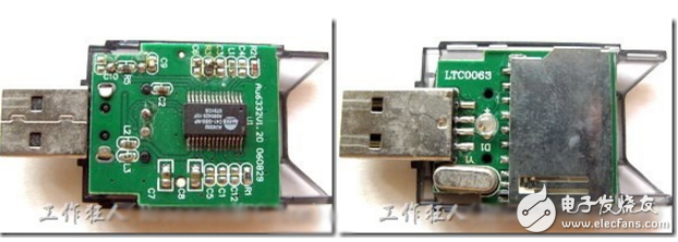
Referring to the front and back pictures of the SD card board at the top of the article, you should be able to make a clear judgment and point out that the side will be arranged on the first side of the part to pass the reflow oven, and that side will be placed in the second Face-to-face patch is over!
In addition, in the mass production of electronic components to be soldered to the board, there are many ways, but each process is actually determined at the beginning of the board design, because its board The placement of the parts will directly affect the welding sequence and quality of the assembly, and the wiring will have an indirect effect.
At present, the welding process of the circuit board can be roughly divided into full-plate welding and partial welding. The full-board welding is roughly divided into reflow soldering and wave soldering (Wave Soldering), while the board is partially soldered with carrier wave soldering ( Carrier Wave Soldering), Selective Wave Soldering, Laser Soldering, etc.
Our 5 wire resistive Touch Screen is the highest accuracy ,stable ,no effect to touch when the liquid pouring or spilling.And it is widely use to Industrial,Retail,
Transportation ,Finance,Hospital or other area.
5 wire touch screen have the following advantages,we worthy of your trust.
1) Can withstand more than 5,000,000 points.
2) 4096x4096 Resolution.
3) USB or RS232 Interface.
4) High accuracy and sensitivity.
5) Glass + Film Material.
6) Finger and touch pen activation.
7) Our products have passed CE, FCC, RoHS certification!
pictures show:


5 Wire Touch Screen Panel,Glass Touch Screen Panel,Touch Screen with Controller,Resistive Touch Screen,Waterproof Touch Screen,GPS Touch Screen
ShenZhen GreenTouch Technology Co.,Ltd , https://www.bbstouch.com