
New Japan Wireless launches broadband low noise amplifier NJG1129MD7
New Japan Wireless launches broadband low noise amplifier NJG1129MD7
New Japan Wireless (Headquarters: Hirata Hirata, President of Chuo-ku, Tokyo) has now completed the development of GaAs MMIC NJG1139UA2, and has begun to supply. This product is a broadband low-noise amplifier with a bypass circuit, which is most suitable for portable digital TV.
ã€Development background】
In recent years, with the increasing number of products that can receive terrestrial digital broadcasts such as portable devices and car navigation systems, in order to improve the receiving sensitivity of the terminal, the market requires low-noise amplifiers with high gain / high linearity / low noise index (later Called LNA). In order to meet the requirements of the market, New Japan Wireless has developed NJG1129MD7 (announced in December 2008). NJG1139UA2 is a wideband LNA GaAs MMIC for terrestrial digital broadcasting developed for easier use by using a miniaturized package based on this, reducing external components.
ã€product features】
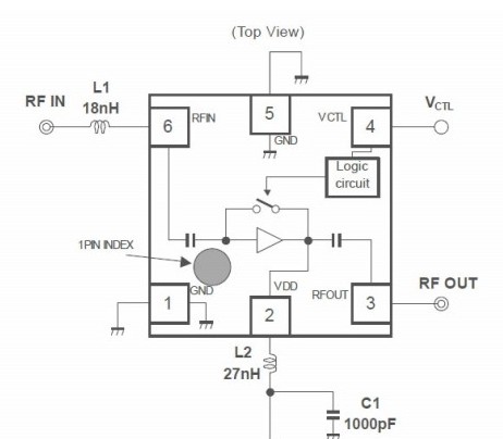
NJG1139UA2 is a low-noise amplifier consisting of a low-noise amplifier circuit, a bypass circuit, and a logic circuit for control. It has the characteristics of high linearity, low current consumption, built-in ESD protection circuit, etc., and in order to prevent the amplifier distortion caused by the strong magnetic field input near the base station, a bypass mode (Low gain) without passing through the amplifier circuit mode).
Feature 1 Space saving due to the use of the latest small package Substrate space.
Feature 2 Due to the low operating voltage and wide operating voltage range of the LNA, it is possible to operate at a low voltage (1.8V typ.), So it can be driven directly from the system power supply.
Feature 3 Reduced defect rate due to high electrostatic pressure resistance performance. Built-in ESD protection circuit realizes high electrostatic withstand voltage. Thereby reducing the bad products caused by static electricity in the manufacturing process of the loading equipment.
ã€other】
・ With bypass circuit mode (High gain mode / Low gain mode)
ã€application】
・ Mobile phone ・ PND
・ PDA
・ Car navigation system and other tuner modules
ã€Product Performance】
・ Broadband: 470 ~ 770MHz
・ Low operating voltage: 1.8V typ. (1.7V ~ 3.6V)
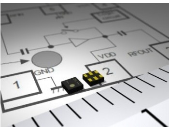
・ Small package: EPFFP6-A2 (Package size: 1.0mm x 1.0mm x 0.37mm typ.)
・ Built-in ESD protection device
[High gain mode]
・ Low current consumption: 3.5mA typ.
・ Low switching current: 6mA typ.
・ Gain: 14dB typ. @ F = 470 ~ 770MHz
・ Low noise: 1.2dB typ. @ F = 470 ~ 770MHz
・ High input P-1dB (IN): -12dBm typ. @ F = 470 ~ 770MHz
・ High input IP3: -4dBm typ. @ F1 = 470 ~ 770MHz, f2 = fRF + 100kHz, Pin = -25dBm
[Low gain mode]
・ Low current consumption: 11mA typ.
・ Gain: -2dB typ. @ F = 470 ~ 770MHz
・ High input P-1dB (IN): + 15.0dBm typ. @ F = 470 ~ 770MHz
・ High input IP3: + 30.0dBm typ. @ F1 = 470 ~ 770MHz, f2 = fRF + 100kHz, Pin = -8dBm
ã€Production plan / Reference price】
Sample supply: Production has started from December 2009: Scheduled to start production in January 2010, 200,000 pieces per month Reference price: Unit price 100 yen
Die casting Zinc Alloy, Aluminum alloy and High Temperature powder coating are applied, which can effectively protect mechanical force and avoid water and powder, provide reliable protection for connected system against severe environment.
Four functions of heavy-duty connector housing:
1. Electrical insulation between connectors to avoid interference between signals.
2. Fixing the position of the connector is conducive to plugging and position stability.
3. Provide mechanical protection and support for the insert
4. Separate the connector from the application environment, reduce the environmental pollution and corrosion of the connector, and extend the service life of the connector
Hood Houses,Connector Hood,Connector Housings,Heavy Duty Connector Housings
Suzhou WeBest Electronics Technology Co.Ltd , https://www.webestet.com