
Ensure that multiple FPGA rails are shut down in the correct order to avoid premature failure of the device due to voltage
Ensuring that multiple FPGA rails are turned off in the correct order is as important as ensuring that the boot procedure is correct, preventing the device from failing early due to undetermined voltage conditions.
Power sequencing avoids damage
There are a number of techniques for controlling the startup sequence and timing when launching multiple rails for today's large system single-chip FPGAs. It is important to follow the correct order specified by the device manufacturer so that the device can be prevented from drawing too much current and causing damage.
Some methods control the Enable pin of the next supply in the sequence by manipulating the power good output of each converter. If a relay is required, a capacitor can be inserted. Another similar approach is to use a reset IC to start the next converter after the previous supply reaches the desired voltage. Each method has some drawbacks, and none of these methods can control the order in which the power is turned off. Closing the rails in the correct reverse order is just as important as turning the power sequence on, just to ensure that the unit operates safely.
With a dedicated power sequencing IC, it is more stable and ensures that the order is correct. The IC can be programmed to transmit the Enable signal at the desired point in time. Figure 1 shows how the multichannel sequencer manages the FPGA core logic, peripherals, and I/O domains. Even so, the power-off sequence is still difficult to control because the decoupling capacitors on each rail may still have residual charge after the converter is turned off, and the residual time is not necessarily the same, and each rail may connect up to 20mF total. Coupling capacitor.
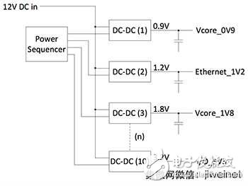
Figure 1 manages the FPGA rails through the sequencing IC.
Sequencer maintains power off control
Using a circuit with a known time constant to actively discharge the decoupling capacitor, the sequencer maintains the correct power-off sequence by temporarily inserting a discharge resistor into the series capacitor. Figure 2 shows how a pair of carefully selected MOSFETs can be used to insert a resistor into a circuit with the addition of the minimum necessary components.
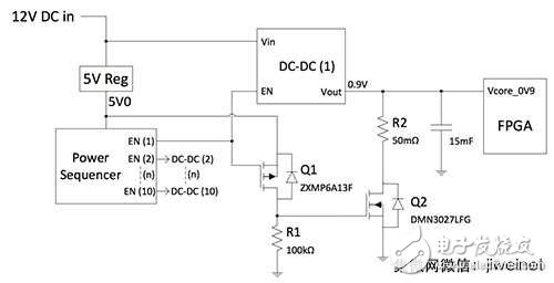
Figure 2 Controls the active discharge circuit for power sequencing.
The EN output of the power sequencer is connected to the Enable pin of the DC-DC regulator and also to the gate of the P-channel MOSFET (Q1). When the sequencer output is reduced and the DC-DC regulator is deactivated, Q1 will reverse the signal and turn on the N-channel MOSFET Q2. When turned on, Q2 will discharge the 15mF decoupling capacitor to ground through the R2 resistor.
The circuit in the figure assumes that the DC-DC regulator cannot continuously produce an output after providing a shutdown signal. If the output of the DC-DC regulator can continue to supply power after receiving a shutdown command, an additional relay is required to activate the discharge circuit.
The selected R2 value must ensure proper discharge time and allow the sequencer to complete the shutdown at acceptable intervals. It should also be noted that the resistance must be large enough to avoid excessive peak current rise rates, avoid EMI problems, and cause transient thermal stress on the Q2 and decoupling capacitor banks. In practice, there are some additional important parameters to consider when selecting the R2 value, such as the on-resistance of R2 (RDS(ON)) and the equivalent series resistance (ESR) of the capacitor bank.
Refer to the output voltage threshold of the power sequencer when selecting MOSFET Q1. The selected device should have a high gate threshold voltage (VGS(th)) to ensure that the sequencer output remains off when the output is high, but note that VGS(th) will rise with the junction temperature. decline. The sequencer operation supply voltage selected in this example is 5V, and the minimum specified high-potential output voltage is 4.19V. Q1's VGS(th) must be greater than 0.9V at 60°C ambient operating temperature to ensure proper operation. In addition, the gate should be pulled down to the source potential with a 100kΩ resistor to avoid accidental opening. Looking at the normalized curve of VGS(th) and temperature in the MOSFET data sheet, it shows that Diodes' ZXMP6A13F meets the requirements: to ensure that the minimum VGS(th) is 1V at room temperature and drops to about 0.9V at 60°C.
In this example, we assume that the sequencer must turn off a total of 10V of power in 100ms. Therefore, the decoupling capacitor bank of each rail must complete the discharge within 10ms. The goal is to achieve three times the RC time constant of 8ms, ensuring that the capacitor discharges to less than 5% of the full voltage within the required time. When calculating the RC constant, the MOSFET RDS(ON), parasitic line resistance, and ESR of the capacitor bank must be considered together with resistor R2.
Assuming that the capacitor ESR and line resistance add up to no more than 10mΩ and the total capacitance of the decoupling capacitor bank is 15mF, the appropriate values ​​for RDS(ON) and R2 can be found using the following equation:
3x (10mΩ+R2+(1.5&TImes;RDS(ON)))&TImes;15mF=8ms
Assuming R2 = 50mΩ, the RDS(ON) of power MOSFET Q2 must be less than 80mΩ at VGS=4.5V and ambient temperature of 25°C.
When choosing a MOSFET, the effects of temperature-dependent changes and the batch variation of RDS(ON) should also be considered. RDS(ON) can vary up to 15mΩ with a 4.5V gate drive and beyond the expected operating temperature range. Therefore, the best practice is to determine that R2 is about twice the maximum RDS(ON) specified by the manufacturer of the selected MOSFET. If R2 is 50mΩ, Diodes' DMN3027LFG N-channel MOSFET can be used. The RDS(ON) typical and maximum values ​​of this device at VGS=4.5V and room temperature are 22mΩ and 26.5mΩ, respectively. Therefore, the RDS(ON) change can be from 15mΩ to 40mΩ, the discharge time starts from 3.9ms with 95% (3 times RC), and the discharge time can be extended to 5.4ms when using the capacitor bank with the worst 20mF size.
Evaluate maximum single pulse protection MOSFET safety
Indoor Cable,Indoor Fiber Optic Cable,Indoor Fiber Cable,Indoor Optical Fiber Cable
Huizhou Fibercan Industrial Co.Ltd , https://www.fibercannetworks.com