
Implementing a parallel/serial conversion circuit using an FPGA
Parallel-serial conversion circuits have a wide range of applications in communication interfaces. Programmable logic arrays are very suitable for parallel and hardware conversion implementations due to their flexibility and reconfigurability. In order to solve the contradiction between resources and performance in hardware circuit structure, three different parallel-serial conversion hardware circuit structures of shift register, counter and combination logic condition are analyzed and compared, and functional verification and performance evaluation are carried out through design simulation. The experimental results show that the implementation method of shift register has the best speed performance. The implementation method of counter has the best cost performance. The implementation method of combinatorial logic condition has the least register resource consumption, which can be reasonably selected according to the actual application requirements. Parallel conversion of hardware circuit implementation.
0 Preface
As an important digital signal transmission path, parallel-serial conversion circuit has a wide range of applications in interface protocols such as SPI, I2C, UART and high-speed SERDES, PCIE and other communication interfaces. In the development of integrated circuits in recent years, there are mainly three ways to design the parallel-serial conversion circuit, which are the design method of integrated circuit customization, the design method based on programmable logic array (FPGA) and the adoption of software. The way of design. The design of parallel-serial conversion circuit based on integrated circuit customization is usually only applied to some applications where the transmission rate is very high, such as 1.25 Gbps parallel-serial conversion integrated circuit and 2.5 Gbps PCIE parallel-serial conversion circuit. 1.25 GHz differential transceiver chip and 4G high-speed parallel-serial conversion circuit. The parallel-to-serial conversion design method of software is usually only suitable for occasions with low transmission rate requirements. At the same time, because the software design method usually takes up the processor time, the performance of the processor is reduced in the case of frequent communication. FPGA-based parallel-serial conversion circuit implementation has achieved wide development due to its good compromise between cost and performance, such as application in interface protocols such as SPI and I2C.
In the FPGA-based parallel-serial conversion circuit implementation, the counter-to-serial conversion circuit is the most widely used method. For example, Sun Zhixiong uses a counter method to implement a 16-bit input/8-bit data output parallel-to-serial conversion circuit. Design and simulation, Wang Chong and so on use the counter method to achieve the 9-bit parallel-serial conversion circuit design, Wang Peng and other methods using the counter to achieve the N-bit parallel-serial conversion circuit design, Xue Peixiang and other methods using the counter to achieve any bit Parallel-to-serial conversion circuit design. Since resource usage and speed are a contradiction in FPGA-based design, how to achieve maximum performance with minimum resources according to specific application requirements is the goal of engineering design.
According to different application requirements, the hardware implementation of different parallel-serial conversion circuits based on FPGA is carried out. The resource consumption and speed performance of three parallel-serial conversion hardware circuit structures are determined by using shift register, counter and combination logic conditions. The function of parallel and serial conversion hardware circuit is verified by design simulation. The experimental results show that the parallel-serial conversion circuit implementation method with shift register has the best speed performance and can be adapted to the field of high-speed applications. The parallel-serial conversion circuit implementation method using the counter has the best performance-price ratio performance, and has the comprehensive ability of resources and speed. The parallel-serial conversion circuit implementation method using combinational logic condition determination has high application value in some cases where the register resources are strictly limited.
1 hardware implementation structure
Resources and performance are a pair of contradictions in the hardware circuit structure. How to design a better hardware circuit structure to make its resources smaller and higher performance has become the goal of researchers. FPGA-based parallel-to-serial conversion circuits have different hardware implementation structures. In order to find an optimal balance between their resource usage and performance, three different parallel-to-serial conversion circuit hardware structures are analyzed and compared, as shown in Figure 1. 2 and Figure 3 are shown.
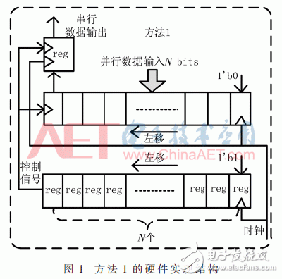
The hardware implementation structure of the parallel-to-serial conversion circuit of method 1 adopts a shift register design scheme. By designing N shift registers and initializing it to 0, a register is left shifted (set 1) every clock cycle to control the serial. The bit width of the output data. This design has fewer combinations of logic design, so the delay of the critical path is theoretically shorter and the speed of the entire hardware circuit is higher.
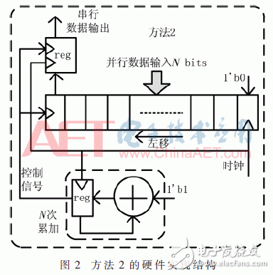
The hardware implementation structure of the parallel-serial conversion circuit of the method 2 adopts a counter accumulation design scheme, and a bit width of the serial output data is controlled by designing a counter having a bit width of log2N for N times of accumulation. This design reduces the amount of register resources used. The critical path is determined by the adder of the combinatorial logic, and the critical path delay is longer than Method 1.
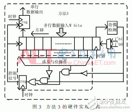
The hardware implementation structure of the parallel-serial conversion circuit of the method 3 adopts a design scheme of the combination logic condition determination, and the bits of the serial output data are determined by bit-and-bit or combination logic determination according to the parity characteristics of the N-bit parallel input data. Wide control. This design scheme is simpler in hardware description language code, and its register resource usage is similar to that of method 2. However, due to the use of more combinatorial logic operations, its critical path delay should be the most in the three methods. long.
Our currency detector or money detector mainly include following models :
1) SLD-16: simple money detector with UV and white light detection
2) SLD-16M: in addition to the function of SLD-16, it has a magnetic head to detect the magnetic ink on notes
3) IRD-ACE: a portable IR detector with chargable battery
4) PF-3000S: a portable multi-function detector with UV IR white light detection
5) MD-8007: a multi-function money detector with UV MG IR white light detection, 7 inch LCD display
6) PF-9007: a multi-function money detector with UV MG IR white light detection, 7 inch LCD display, has two built in cameras. one is for checking whole image, the other is for checking partial image
Banknote Discriminator,Money Detector,Currency Detector,Compact Uv Money Detector
Suzhou Ribao Technology Co. Ltd. , https://www.ribaoeurope.com