
High-precision ADC board layout and wiring case
When designing a high-performance data acquisition system, diligent engineers carefully select a high-precision ADC and other components needed to simulate the front-end regulation circuit. After a few weeks of design work, simulations were performed and schematics were optimized, and in order to get busy, designers quickly assembled board layouts. A week later, the first prototype board was tested. Unexpectedly, board performance is not as expected.
Optimal PCB layout is important to get the ADC to the desired performance. When designing a circuit that includes a mixed-signal device, you should always start with a good grounding arrangement and divide the design into analog, digital, and power sections using the best component placement and signal routing traces.
The reference path is the most critical in ADC placement and routing because all conversions are a function of the reference voltage. In the traditional successive approximation register (SAR) ADC architecture, the reference path is also the most sensitive because there is a dynamic load on the reference pin to the reference source.
Since the reference voltage is sampled several times during each conversion, a high current transient occurs on the terminal where the ADC internal capacitor array is turned on and charged when this bit is set. The reference voltage must remain stable for each conversion clock cycle and settle to the desired N-bit resolution, otherwise linearity errors and missing codes may occur.
Figure 1 shows current transients during the conversion phase on a typical 12-bit SAR ADC reference terminal.
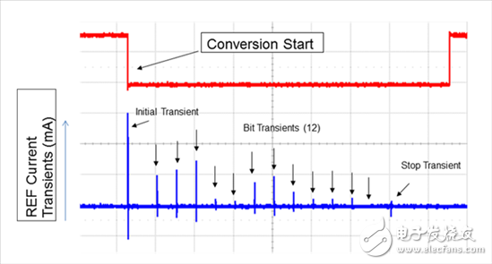
Figure 1.12 Current Transient on Bit of SAR ADC Reference Pin
Due to these dynamic currents, a high quality bypass capacitor (CREF) is required to decouple the reference pin. This bypass capacitor is used as a charge store to provide instantaneous charging during these high frequency transient currents. You should place the reference bypass capacitors as close as possible to the reference pins and connect them together using a short, low-inductance connection.
Figure 2 shows an example of board layout for the ADS7851, a 14-bit dual ADC with two independent voltage references.
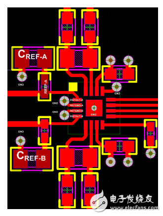
Figure 2. Dual ADC Place and Route Example with Two Independent Internal Voltage References
In this four-layer PCB board example, the designer used a solid ground plane directly below the device and divided the board into analog and digital sections to keep sensitive input and reference signals away from noise sources. He bypasses the REFOUT-A and REFOUT-B reference outputs with a 10μF, X7R, 0805 ceramic capacitor (CREF-x) for optimum performance and connects them to devices using small 0.1? series resistors. To maintain a constant impedance at low overall impedance and high frequency; he also uses wide traces to reduce inductance.
I highly recommend placing CREF on the same layer as the ADC. You should also avoid placing a via between the reference pin and the bypass capacitor. Each of the reference ground pins of the ADS7851 has a separate ground connection, and each bypass capacitor has an inductive connection to the ground path.
If you are using an ADC that requires an external reference, you should minimize the inductance in the reference signal path - the starting point of this path is the reference buffer output to the bypass capacitor until the ADC reference input.
Figure 3 shows an example of the placement and routing of an 18-bit SAR ADC ADS8881 using an external reference and buffer.
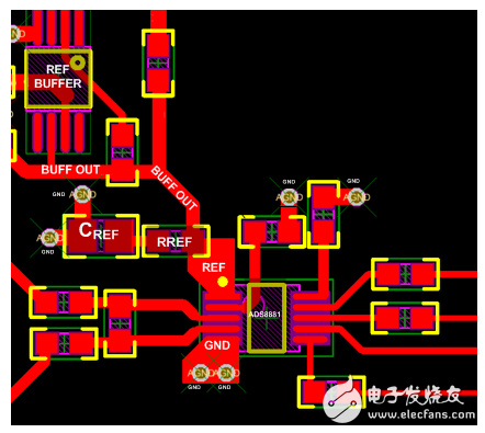
Figure 3. Example of ADC layout with an external reference and buffer
By placing the capacitor within 0.1 inches of the pin and connecting it to a 20 mil wide trace and multiple 15 mil ground vias, the designer places the reference capacitor between the REF pin and the REF pin. The inductance is maintained at a level of less than 2nH. I recommend using a single, 10uF, X7R, 0805 ceramic capacitor with a rated voltage of at least 10V.
The trace length of the reference buffer circuit to the REF pin is kept as short as possible to ensure fast and stable response.
Proper decoupling of the REF pin is critical to achieving optimal performance. In addition, maintaining a low-inductance connection in the reference path keeps the reference drive circuit stable during the conversion process, allowing you to take another step toward achieving the desired results.
The touch screen monitor allows the user to operate the host computer simply by touching the icon or text on the computer display screen with his finger, thus getting rid of keyboard and mouse operations and making the human-computer interaction more straightforward. Mainly used in information inquiry in public halls, leading offices, electronic games, song and order, multimedia teaching, air ticket / train ticket pre-sale, etc. The products are mainly divided into three types: capacitive touch screen, resistive touch screen and surface acoustic wave touch screen.
touch monitor,touch screen monitors,touch screen display,touch monitoring,touch monitor price,touch monitors for pc
Shenzhen Hengstar Technology Co., Ltd. , https://www.angeltondal.com