
Electronic Technology Decryption: Simplified FPGA Power Supply Design
FPGA is a field programmable gate array. It is a chip with multiple power requirements. When electronic chips are common in electronic technology design, the power supply design requirements are also strict when powering them. Multi-power supply design is complicated. We need to simplify the power supply design and save cost when FPGA is running efficiently. The following is the specific power supply design method.
FPGA is a multi-power requirement chip with three main power requirements:
1.Vccint core working voltage
Generally, the voltage is very low, and the currently used FPGAs are all around 1.2V. Powering the various logics inside the FPGA, the current varies from a few hundred milliamps to a few amps, depending on the operating clock rate of the internal logic and the logic resources it occupies. For this power supply, a high capacitive impedance during load requires high transient response to the power supply, and because of the low operating voltage and high operating current, it is very sensitive to the wiring resistance of the PCB. Special attention should be paid to the trace width. Reduce the losses caused by wiring resistance.
2.VccoI/O drive power supply
FPGAs often communicate with a variety of different level interface chips, so they usually support a very large number of level standards. Vcco is powering the I/O drive logic of the FPGA. Different level standards require different I/O voltages. For details, please refer to the FPGA related chip manual. For example, XilinxSpartan6 series, you should consult the Xilinx official document, number ds162.pdf, which is detailed in page7table7RecommendedOperaTIngCondiTIonsforUserI/OsUsingSingle-EndedStandards. In addition, in order to communicate with a variety of different standard interface chips at the same time, Vcco is usually independent of BANK, which means that there are several different I/O voltages on one FPGA chip. Of course, there can only be one I/O voltage in the same BANK.
3.Vccaux auxiliary power supply
FPGA is not a pure digital logic chip. It also has some analog components inside, such as Xilinx's DCM digital clock management component. These analog components have power supply rejection ratio (PSRR), which is power supply noise, or power supply pattern. Waves are very sensitive, so a separate power supply is usually used. The current demand of this power supply is generally not large, but the noise tolerance to the power supply is very low. Therefore, the power purity should be improved as much as possible. For example, if you do not directly use the switching power supply, first use the LDO regulator and then supply Vccaux. In addition, Vccaux also supplies some I/O power, such as function selection pins, JTAG, etc., please refer to the power supply instructions of the chip manual.
Since there are so many power requirements, then some problems in power supply design have to be considered when designing the power supply.
There are several power supply design issues to consider when powering an FPGA:
1. Increased the number of output voltage rails
2. Need to set the set point accuracy for the power rail
3. Need to optimize the passive board layout in the design to achieve very low ripple noise
4. Requires AC transient response and compensation loop
Also, don't forget to have sorting and more features you need.
Figure 1 shows a typical FPGA power solution in an FPGA development kit. In addition to choosing the right device and inductor, the design requires some additional expertise. For example, you need to consider the details of component placement and board layout.
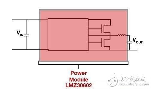
Figure 1. Typical FPGA Power Solution
So how can you simplify the power supply design?
Fortunately, there are a variety of solutions that help simplify. Highlight two innovative technologies that can help you achieve your design goals quickly and easily.
Simplify power supply design method one:
The technology to be highlighted is the WEBENCHFPGAArchitect design tool for creating FPGA power solutions (principle design plus simulation results)
The WEBENCHFPGAArchitect design tool can help you:
Choose the FPGA vendor you want and choose the FPGA product family you will use to meet the power requirements defined by the FPGA Power Estimator tool provided by the FPGA vendor.
Perform these simple steps to achieve an FPGA power solution and optimize it in terms of product size, efficiency and cost. This easy-to-use tool can help you overcome your initial obstacles and reduce your design time from days to minutes to gain a lead.
Simplify power supply design method two:
It is an integrated inductor power module that simplifies the design.
Power modules primarily integrate inductors in a single IC package, but can also integrate other external components such as FETs, compensation loops (if needed), and feedback resistors. Power modules are very versatile, such as enabling and power-good pins for sequencing, and requiring minimal external components such as input capacitors, output capacitors, and possibly a feedback resistor. This module helps to simplify the power solution of Figure 1 to the solution of Figure 2. An integrated inductor power module can be used to power the FPGA and is considered a suitable power solution by FPGA vendors. In addition, these modules help simplify board layout and help you complete designs faster than ever before.
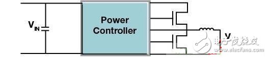
Figure 2. Integrated inductor power module with LMZ30602
Air Pump For Volleyball,Volleyball Hand Pump,Mini Hand Ball Pump,Pump For Volleyball
SHENZHEN SMARTNEWO TECHNOLOGY CO,. LTD , https://www.newopump.com