
LED driving technology for reducing the power consumption of LCD TVs
According to the Super Energy Efficient Equipment and Appliances Promotion (SEAD) project, TV energy consumption accounts for about 3% to 8% of the electricity consumed by the global population. Research conducted by Lawrence Berkeley Labs believes that using advanced technologies such as more efficient LED drivers will significantly reduce the energy consumption of televisions.
This article refers to the address: http://
There is little doubt that liquid crystal display (LCD) technology with LED backlighting is the only viable way to achieve the efficiency goals recommended by the authorities. The disadvantage of plasma TVs is that each pixel is an active illuminator, so its power consumption is directly proportional to the number of pixels. At the same resolution and brightness, HD plasma TVs consume approximately two to three times as much power as LCD displays. The widely publicized OLED technology is not listed so fast, and the investment required for this "extremely cutting edge" large-screen technology is enormous. However, the use of the most advanced TFT-LCD technology and large display with "smart" direct LED backlighting and local dimming is much cheaper than OLED, while power consumption and image quality are similar.
However, current LCD TVs, including LCD TVs that use LED backlighting, still have a certain gap with the efficiency goals they will achieve in the next few years. However, the latest LED driver circuit design technology has significant energy-saving effects and can play a far-reaching role in helping TV manufacturers meet stringent power requirements.
Changing TV power consumption standards
The ENERGY STAR TV power consumption standard was introduced in 2008, and the TV power consumption indicator in this standard will continue to decrease every year. Since the maximum power consumption allowed by the current standard is 85 watts regardless of the size of the TV set, the design challenge will be even more daunting for large-screen TVs.
Although ENERGY STAR is a spontaneous standard, it has a lot of influence and is not the only one. For example, the California Energy Commission has issued its own standards. Their standard is stricter than the ENERGY STAR standard and has a lot of lethality - it prohibits the sale of TV sets in the California region that do not meet their energy efficiency targets. In Europe, regulations have been enacted for many years, allowing direct comparisons of white goods' energy consumption (EU energy label), which consumers often use as a basis for purchasing decisions. These regulations are now mandatory for TVs, cars and other products.
How LED backlighting works
Since LED backlighting consumes about 30% to 70% of the total system power consumption of LCD TVs, improving the efficiency of backlighting circuits has a considerable effect on improving system efficiency. As is often the case in power system design, many inconspicuous efficiency improvements can be combined to achieve significant energy savings.
There are two main ways to implement LED backlighting (see Figure 1). In an indirect or edge-lit backlighting scheme, LEDs are placed at the edge of the screen and light is evenly distributed throughout the display through the light guide. This solution has good optical uniformity in screens up to 40 inches, and the backlight components are only 5mm to 10mm thick.
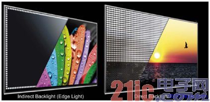
Figure 1: LCD TVs can use one of two LED backlighting methods.
In a direct backlight system, the LEDs are placed directly behind the LCD, with low power consumption, good thermal design, and excellent scalability, especially with no restrictions on screen size. The thickness of this type of screen is usually thicker than that of the edge-lit screen, but with the latest lighting technology, the thickness of this display can now be 8mm. An important advantage of direct backlighting is that it enables complex local dimming, which reduces power consumption and improves dynamic contrast, making the latest TV designs comparable to OLEDs.
Architectural choice of LED backlight system
Designers typically choose the architecture of the LED backlight drive system based on maximum energy savings and significantly enhanced image quality standards. In addition, designers want to strike the best balance between locally controlling LED strings and the lowest bill of materials (BOM) costs.
Single string and single DC/DC converter
This solution uses a Switching Power Supply (SMPS) to supply voltage to a string of placed backlights and a current sink to regulate the current flowing through the LED strings. In order to minimize power consumption, the voltage requirement at the ILED current sink is a little higher than the required voltage to ensure that the LED can receive the specified current (see Figure 2).
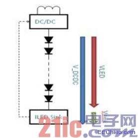
Figure 2: Back-illuminated system architecture for a single-string, single DC/DC converter.
A common design method is to establish a feedback path from the ILED current sink to the switching Power Supply to regulate the output voltage of the switching power supply. This feedback path establishes a change in the forward voltage (Vf) that exists between different LEDs. The white LED has a typical Vf of about 3.2V, but different LED variations can be as high as ±200mV. Therefore, in a string of 10 LEDs, the total VLED voltage value may be in the range of 30V to 34V.
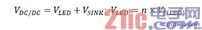
The output voltage required by the DC/DC converter can be expressed as:
Assuming VSINK is 0.5V, the ILED current sink must adjust the VDC-DC to 30.5V to 34.5V, depending on the actual LED forward voltage.
Multiple strings and multiple DC/DC converters
A single string of LEDs is rarely sufficient, as the output voltage of the DC/DC converter increases as the number of LEDs in the string increases. After VOUT/VIN exceeds a certain ratio, the efficiency of the switching power supply drops dramatically. Therefore, LED backlight designers can use multiple LED strings to avoid excessive voltage output from the switching power supply.
The easiest way is to duplicate the topology of a single string of single DC/DC converters per string (see Figure 3). The advantage of this method is that it is efficient because the voltage of each string can be adjusted separately. The disadvantage is the high cost because each string requires its own DC/DC converter, MOSFET, coil, diode and output capacitor. To save BOM cost, designers can reduce the number of LED channels by using long strings, using more LEDs in each string. But this method sacrifices the system's ability to achieve local dimming, which is another important energy-saving technology. So this topology will not be particularly attractive anyway.
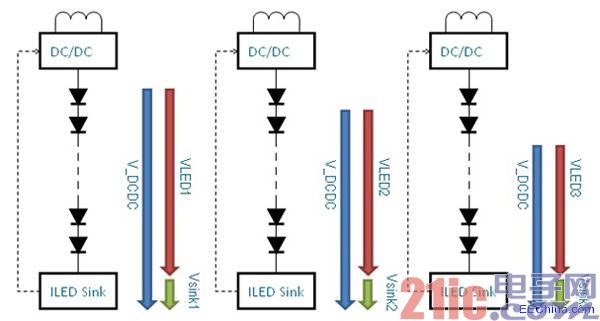
Figure 3: Using a separate DC/DC converter for each LED string is an expensive solution.
Multiple strings using one DC/DC converter
Multiple strings plus a single DC/DC converter topology is a better way to reduce BOM cost (see Figure 4). The disadvantage of this method is that the voltage of the switching power supply must be adjusted to be higher than the LED string with the largest forward voltage, which means that the operating voltage of the system is higher than the voltage necessary for those strings with a lower forward voltage. This means that the ILED current sink must consume too much power from the LED string with a lower forward voltage, which creates excessive heat that must be dissipated from the board, reducing energy efficiency.
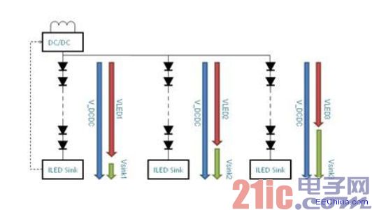
Figure 4: The voltage of the switching power supply is not optimal when using a DC/DC converter to connect multiple LED strings.
Multi-string hybrid architecture
An architecture that combines multiple strings of components and multiple DC/DC converters provides the best balance between efficiency and BOM cost. This hybrid architecture (see Figure 5) has multiple DC/DC converters that power the LED string set.
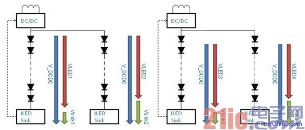
Figure 5: A hybrid architecture can strike the best balance between BOM cost and energy efficiency.
This solution offers the highest overall energy efficiency because it combines the local dimming advantages of a direct backlight system with good DC/DC output voltage regulation, as well as efficient multiple strings, multiple DC/ The DC converter architecture provides true BOM savings.
Adjust the current to match the characteristics of the LED
LED manufacturing processes can cause large variations in brightness and color temperature between different LEDs. For the convenience of the user, the white LED manufacturer assigns each manufactured unit to an LED group or "box" that performs equally well in terms of color, brightness, and forward voltage. However, the specifications set by the manufacturer for each brightness and color oven are only valid under certain nominal operating conditions. This means that the LED current must be set to the nominal current specified in the data sheet to produce the specified brightness and color.
As a result, the dimming and brightness control functions can only be achieved by switching the current of any of the LEDs to a conducting (nominal current) or a shutdown (zero current) state via a digital PWM control signal. During analog dimming, the LED will operate outside of the specified nominal current range, which will result in unacceptable color temperature variations and poor LED-to-LED brightness matching (see Figure 6).
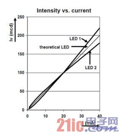
Figure 6: LED brightness from the same box is guaranteed only at nominal current (20 mA in this example).
Current slot characteristics
Since the LED requires a completely stable constant current power supply, the main function of the LED driver is to set the current to a nominal value when turned on and to set the current to 0A when turned off. Thus, a feedback loop that controls the adjustment accuracy requires the use of a particularly precise current sink (see Figure 7).
Although there are various current slot designs on the market, the high precision requirements of TV backlighting (current regulation is higher than ±0.5%) require the use of precision op amps to set the ILED current independent of the ILED voltage. However, in backlight driver applications, the task is more challenging because the accuracy of the current adjustment must be maintained even if the voltage of the current sink is reduced to very small.
This is a difficult requirement, but AMS's four generations of high precision current slot LED drivers - the AS369x, AS381x, AS382x, and AS385x - are specifically designed for this application. These devices also use offset-compensated op amps. The current sink driver requires the drain to be at a minimum voltage (VDS(sat)) to ensure that the current sink transistor has full accuracy in the saturation region and is able to operate properly. In the saturation region, the gate-to-source voltage is primarily used to control the output current.
If you want the current sink to work efficiently, it is important that the voltage drop between VSET and VDS is low. LED drivers with op amps and built-in offset cancellation maintain VSET levels as low as 125mV to 250mV. In order for the VDS to have an extra margin of more than 150 mV of VDS(sat), the total voltage drop of the current sink must be around 400 mV. For strings with 8 LEDs (Vf? = 8 x 3.2 = 25.6 V at this time), the power loss in ISINK is approximately 1.5%. When the offset cancellation function is not included in the AMS backlight LED driver, the value of VSET will be higher, which will result in more power loss in the current sink.
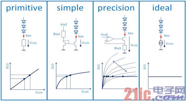
Figure 7: Current Slot Design; Precision Current Slot requires a precision op amp with offset compensation.
Feedback adjustment mechanism for optimizing power consumption
As indicated above, the feedback path established from the LED driver to the switching power supply sets the drain voltage to the minimum required value. The output current sink can be implemented with a simple and mature current output driver plus an external capacitor (see the left panel in Figure 9), or a digital control circuit that can set the start/release time and use a digital-to-analog converter to control the current output. To achieve (IDAC) (see the right image in Figure 8).
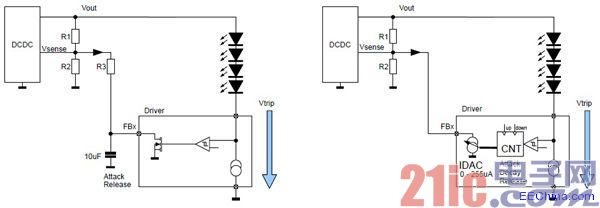
Figure 8: Two different implementations of the feedback loop to the switching power supply.
Both solutions are highly efficient, can use a variety of switching power supplies with voltage feedback loops, and can be achieved by connecting the feedback loop from more than one drive to the same switching power supply. This is the hybrid architecture system. Requirements.
However, the second digital implementation has some specific advantages. In addition to not requiring the use of output capacitors, this digital circuit allows designers to freely define the start-up and release times of the feedback system. By choosing a combination of fast start-up time and a combination of release delay and relatively slow release, the performance of the display can be significantly improved. This benefit is especially noticeable where high brightness changes are required. In this case, the quick start time can eliminate the perceived brightness 当 when the screen changes from dark to full light. The analog solution (see Figure 8) gradually adjusts the LED output during a short dark frame, so there is a visible delay for the next bright frame to reach full brightness.
This phenomenon can distract TV viewers because of the large dynamic range between frames and frames of movies and other video content. This trick can be eliminated with a digital adjustment circuit by inserting a delay of a few hundred milliseconds during the release operation. Thus, when a bright frame is interrupted by a series of short dark frames, the second bright frame will start from full light because the driver will automatically delay the voltage drop process. A digital feedback algorithm that enables release delay is used in AMS products.
Another useful feature integrated in the LED driver IC is the Fast Serial Peripheral Interface (SPI). In direct-backlit TVs, LEDs are arranged in a large number of relatively short strings, so a small-sized display can achieve energy savings by dimming the light. Typically this arrangement contains 256 channels in a 16x16 field matrix, each of which can be individually configured by Pulse Width Modulation (PWM). But using 256 PWM signals with variable PWM width and delay is a task that consumes a lot of processor resources, and even the fastest microcontrollers can be overwhelmed.
Therefore, these backlighting systems use a PWM generator integrated in the LED driver IC so that the brightness can be configured by simple SPI data transmission. In an architecture with multiple driver ICs (eg, 16 channels per IC, a total of 16 ICs with 256 channels), the LED channel can be daisy-chained by SPI signals and the data used in the VSYNC frame is transferred to the previous one. The frame is configured.
In this scheme, the data transmission speed through the SPI can reach 20 Mb/s, or reach 50 kb/frame at the 400 Hz frame rate. This speed is fast enough to change the dimming effect of each field at the speed of synchronizing the actual frames. Therefore, ideal local dimming can be achieved with very little microcontroller overhead.
Intelligent dimming function for edge lighting systems
This local dimming technique can only be used in direct backlighting systems, but some specific smart dimming techniques can also be implemented in edge lighting systems. Especially PWM dimming, it can change the brightness without changing the color temperature of the white LED. Unlike the edge illumination LED being permanently set to a specific brightness value, the brightness can be dynamically changed by changing the pulse width.
Another energy-saving technology is called Dynamic Brightness Adjustment (DLS). With this technique, the white/luminance value of the LCD can be increased in some cases, allowing the power output of the backlight LED to be reduced.
Using ambient light sensors (ALS) is another way to reduce power consumption. If the room light placed in the TV is quite dark, you can reduce the brightness of the backlight (see Figure 9).
Figure 9: Energy-saving method using smart LED drivers and smart ALS sensors.
TV manufacturers are studying more complex methods. For example, the camera begins to enter the display design, which allows consumers to use video telephony services such as Skype on their TVs. These cameras can also be used to detect if someone is actually watching TV. If the TV is on, but no one is in the room, the backlight can be automatically reduced to the lowest brightness.
Even custom energy consumption modes can be implemented. While you may prefer to watch TV in an energy-friendly eco mode that reduces backlight brightness, other members of the home may prefer to watch it.
In short, significant energy savings can be achieved by implementing the current advanced high-efficiency LED drive technology. The importance of this technology will become more and more important as more stringent regulations continue to reduce the maximum power that new TV sets are allowed to consume.
APM Lab DC Power Supply is designed to provide continuously variable output voltage and current for a broad range of applications in a compact 1U and 2U high ,19" standard rack mounting. The front panel layout makes the Laboratory DC Power Supply easy to use.
Some features of the High Voltage DC Power Supply as below:
- Ultrafast respond time and high efficiency
- Accurate voltage and current measurement capability
- Constant Power and wide range of voltage and current output
- Equips with LIST waveform editing function
- Compliant with SCPI communication protocol
- Support RS232/RS485/LAN/USB (standard) ,GPIB (optional)
- Master/Slave parallel and series operation mode for up to 10 units
- Built-in standard automobile electrical testing curves
- Full protection: OVP/OCP/OPP/OTP/SCP
- Voltage drop compensation by remote sense line.
- Have obtained CE,UL,CSA,FCC.ROHS
200V DC Power Supply,DC Switching Power Supply,Adjustable Power Supply,Digital Control Dc Power Supply
APM Technologies (Dongguan) Co., Ltd , https://www.apmpowersupply.com